Home

Results of the Project

Themes of the Project


Quantum Chemical Simulation: The Next Generation

Quantum Molecular Interaction Analysis

Nano-scale Device Simulation

Fluid Dynamics Simulation: The Next Generation

Structural Analysis: The Next Generation

Platform of Problem Solving Environment

High-Performance Computing Middleware

Outline of the Project

Personnel


IIS

Link

Site Map


Internal Access


Collabolative Research Center of Frontier Simulation Software for Industrial ScienceInstitute of Industrial Science, University of Tokyo4-6-1 Komaba, Meguro-ku, Tokyo 153-8505, Japan

Nano-scale Device Simulation


Software
Researchers


A nano-scale simulation system based on the first principles techniques predicts and designs the materials properties and functions necessary for the next-generation semiconductor nano-devices
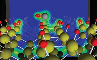
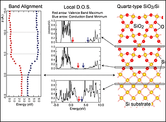
In order to develop the next-generation semiconductor nano-devices, we have to make a drastic breakthrough in science and technology for surfaces and interfaces fabricated in nano-meter length scale. Especially, fabrication and control of interface structures in nano-meter length scale, materials design of good-quality high-k dielectrics for gate insulator films, and analysis of electronic transport properties in nano-scale interfaces are crucial to the development of silicon-based nano-devices.
Investigation of exotic properties and functions which other nano-scale structures than silicon-based ones may exhibit, and the knowledge of fabrication of such a nano-scale structures with a given function are also of great importance.
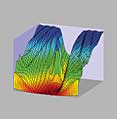
In this project, we are aiming to develop a nano-scale device simulation system to precisely analyze and predict the structures, properties, and functions of nano-scale materials, by mainly using first-principles electronic-structurecalculation methods.


Image1
Adsorption of a Si atom on a hydrogen-terminated Si(001) surface. interaction analysis system.


Image2
Electronic states of a single atom sandwiched between two metallic electrodes.


Image3
Band alignment for a SiO2/Si interface.


Page Top


Copyright