Process simulation of carbon based nanostructures in next-generation semiconductor integrated elements
- Theme Leader
- Takahisa Ohno Director-General, Computational Materials Science Unit, National Institute for Materials Science
- Alliance for Research
- Yasunari Zempo Professor, Graduate School of Computer and Information Sciences, Hosei University
- Takeo Hoshi Associate Professor, Graduate School of Engineering, Tottori University
- Satoshi Itoh Coordinator, RIKEN Advanced Institute for Computational Science
- Chioko Kaneta Fujitsu Laboratories Ltd.
- Hiroyuki Kageshima Senior Research Scientist, NTT Basic Research Laboratories
Research and Development to Accomplish the Strategic Goals
【Overview】
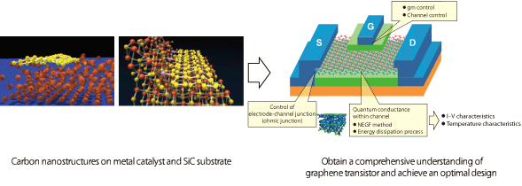
For the future downsizing of semiconductor devices, there is a need for novel materials and manufacturing processes that go beyond conventional approaches. This study aims to support research and development in industrial innovation by creating a knowledge base on the nanostructure processes of carbon materials and other non-silicon materials, which should be applied to channels and wires in semiconductor devices of nanoscale generation.
【Specific Research Targets】
1) Development of optimal process design technology for next-generation nanostructure materials
Using first-principles electronic structure analysis software (PHASE) as the base software, we analyze the electronic structures of carbon based materials and other non-silicon materials, and design nanostructure materials that are appropriate for channels and wires in next-generation semiconductor devices. We will newly implement preprocessing and postprocessing functions using PHASE to assess ohmic junction formation between channel materials and substrate/electrodes. Thereafter, we will propose guidelines for the optimal design of nanostructures.
2) Comprehensive investigation of semiconductor characteristics of carbon nanostructures
We will theoretically calculate the current/potential characteristics of nanostructure materials and quantitatively estimate the effects of impurities and lattice mismatches. In addition, we will analyze the electrical conductivity and electronic states of the junctions between nanostructure materials and substrate/electrodes, which are critical when using nanostructure materials for wires and channels. We will comprehensively assess the potential of these analyses as tools for designing channel structures.
3) Creating a knowledge base on carbon nanostructure materials and providing it in industry-friendly form
We will provide an industry-friendly simulation environment that combines software tools ranging from first-principles atomic/electronic structure analysis programs to modeling and visualizing applications, together with their effective usages, which are studied in this R&D project.
Software: PHASE


